
1. Introduction
This document is an accompaniment to the Shimmer3 JTAG Developer Board whose aim is to aid the user in getting started with the product.
Shimmer3R: The Shimmer3 JTAG Developer Board is for Shimmer3 only. It provides JTAG and Spy-Bi-Wire access to the Shimmer3’s MSP430 processor, which a Shimmer3R does not have. Shimmer3R’s STM32 processor is programmed and debugged over SWD (for example with an ST-LINK and STM32CubeIDE), and customers update its firmware over USB with Consensys.
A Shimmer3R’s SWD port is reached only by opening the unit and attaching a debugger to the 6-pin needle connector on its board. Opening the unit invalidates its warranty.
The Shimmer3 JTAG Developer Board enables users to incorporate additional functionality to the Shimmer3 by providing access to develop their specific application to their own user requirements. It facilitates in-system programming and debugging of the Shimmer3 – via a standard JTAG connection – to aid in the development of custom firmware solutions.
In addition, the Shimmer3 JTAG Developer Board allows for prototyping of 3rd party sensors or custom sensing solutions with the Shimmer3 by facilitating access to each of the pins from the Shimmer3 external connector, thus enabling an Analog Output Sensor, a Digital Output Sensor, a Serial UART or a Parallel Bus Interface to connect to the Shimmer3.
The Shimmer3 JTAG Developer Board is normally connected in-line between the external connector of a Shimmer3 and the Shimmer Dock. An on-board mode selection switch allows the user to easily switch between the standard Bootstrap loading functionality of the Shimmer Dock or JTAG Programming Mode. Alternatively, the board can be powered directly via a built-in Mini-USB connector, for use without a Shimmer Dock.
2. General Information
2.1. Pre-Requisites
- A Shimmer3 device programmed with appropriate firmware, either stock or custom built.
The Shimmer3 stock firmware, LogAndStream, logs to the SD card and streams over Bluetooth. Its source is at https://github.com/ShimmerResearch/shimmer3-firmware, and releases are published there. The latest version should always be used.
A Shimmer3 JTAG Developer Board.
An MSP430 FET, such as the Texas Instruments MSP-FET430UIF or equivalent from another manufacturer (e.g., Elpotronic).
Code compiling software which supports the MSP430F5437A microcontroller (e.g., Code Composer Studio™).
A Shimmer Dock or Mini-USB power cable.
2.2. Expansion Board Features
Full JTAG programming and in-system debugging capabilities.
Easy access to multiple Shimmer3 microcontroller signals using through-hole solder pads.
Connection with an auxiliary power supply.
A hard-wired Shimmer3 reset push button.
2.3. Basic Overview
The Shimmer3 JTAG Developer Board, shown in Figure 2‑1, can be used by firmware developers for debug and programming purposes. It can also be used to provide access to several input/output pins of the Shimmer’s microcontroller for peripheral prototyping. The board can be installed in-line with the Shimmer Dock to enable use of 3rd party JTAG programming and debugging tools.
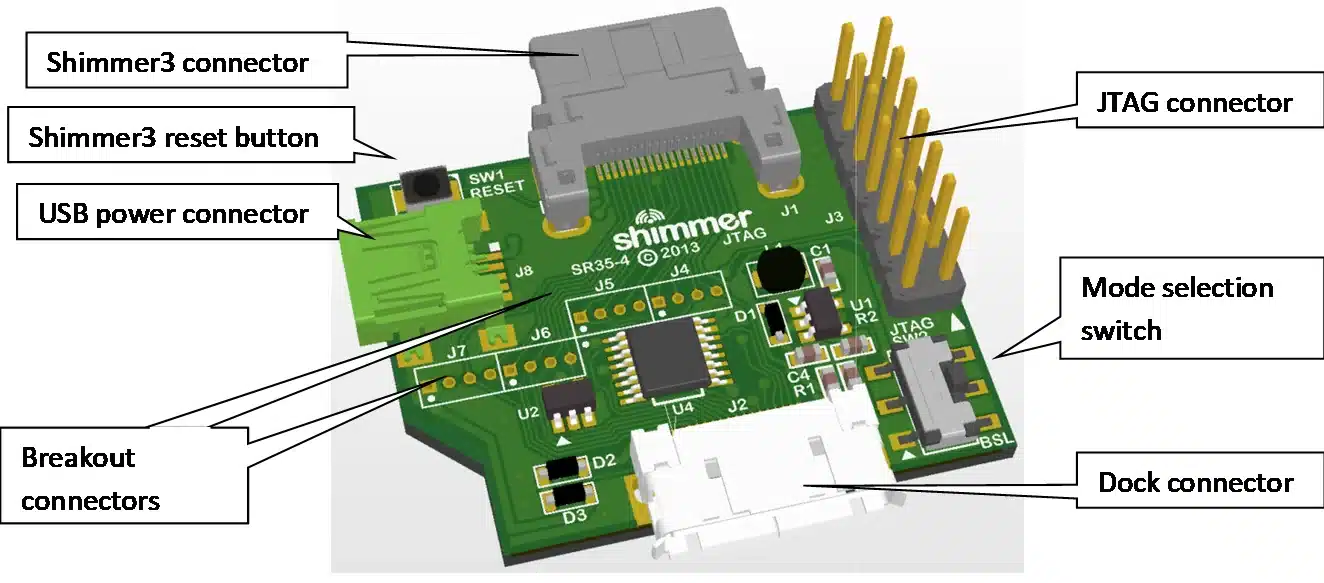
Figure 2‑1: The main features of the Shimmer3 JTAG Developer Board.
| (a) Shimmer Dock powered | (b) Mini-USB powered |
|---|---|
 |
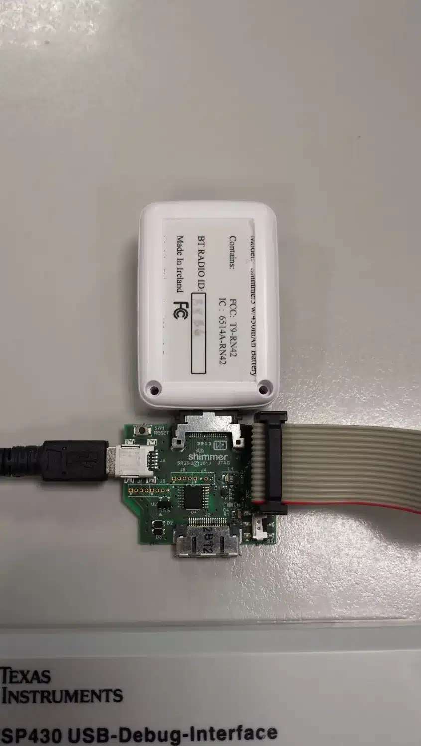 |
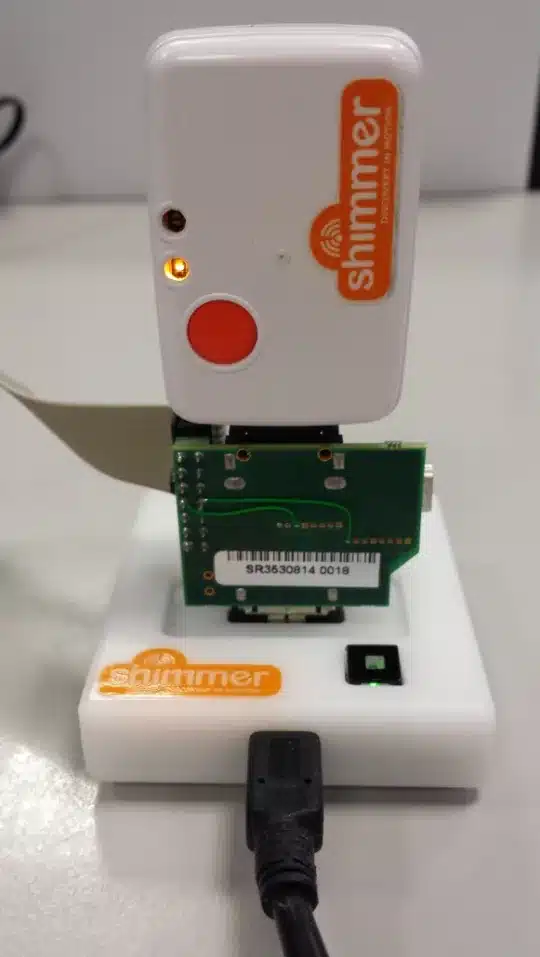
Figure 2‑2: The Shimmer3 JTAG Developer Board should be powered by either the (a) Shimmer Dock or (b) the on-board Mini-USB connector.
The “Shimmer3 connector”, labelled in the Figure 2‑1, should be inserted into the Shimmer3 external connector and the “Dock connector” should be connected directly to the Shimmer Dock, see Figure 2‑2 (a). Alternatively, the board can be powered directly via the USB power-only connector, for use without a Shimmer Dock, as shown in Figure 2‑2 (b). Please note that when undertaking firmware development involving microSD card access (as is the case with SDLog development), the developer board must be powered by the on-board USB connector and not through the Shimmer Dock.
2.4. Mode selection switch
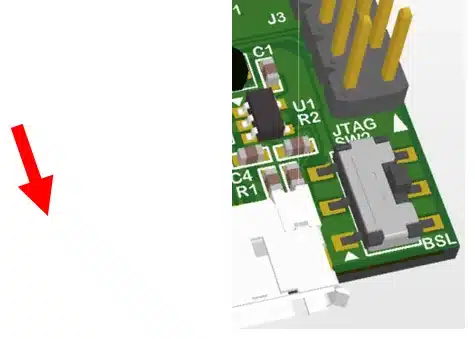
When used in conjunction with a Shimmer Dock, the mode selection switch on the Shimmer3 JTAG Developer Board (as shown in Figure 2‑3) facilities fast switching between normal docking mode operations (such as microSD card access or Bootstrap loading) and JTAG programming mode. When the mode-selection slide switch is down (i.e., towards the “BSL” PCB label), the device is in normal dock operation with the JTAG operation and connector disabled. When the switch is up, JTAG operation is enabled and the Shimmer Dock is only utilised to power the JTAG developer board.
| (a) Normal Dock Mode | (b) JTAG Programming Mode |
|---|---|
 |
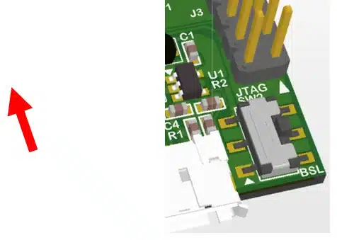 |
Figure 2‑3: Mode selection switch actions – (a) Normal Dock Mode for and (b) JTAG Programming Mode
If the JTAG developer board is powered by the Mini-USB instead of the Shimmer Dock, the mode selection switch need just be placed in the JTAG programming mode position.
2.5. Board Layout
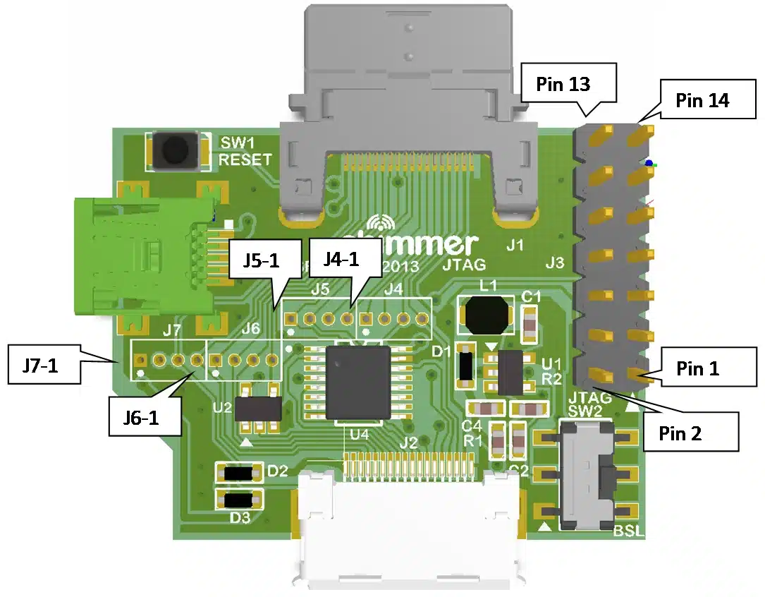
Figure 2‑4: Shimmer3 JTAG Developer Board Top View
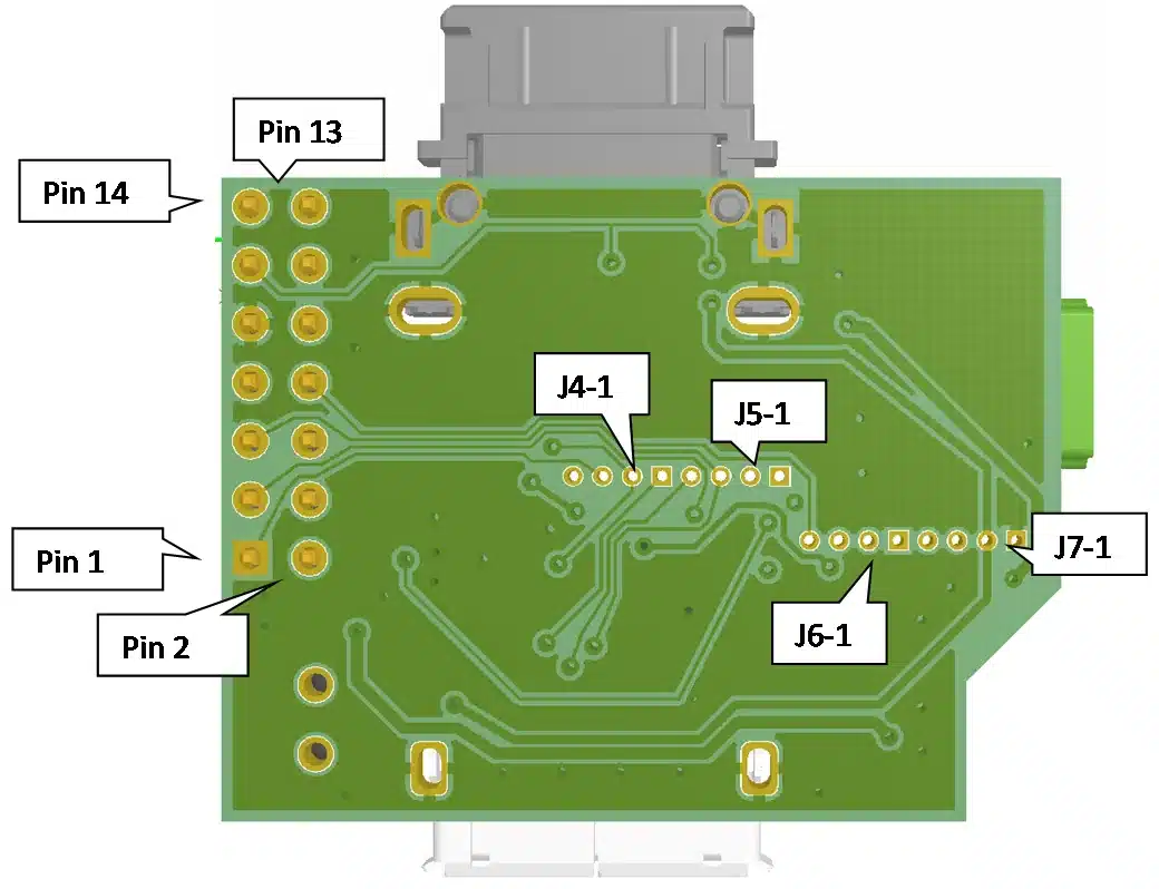
*Figure 2‑5: Shimmer3 JTAG Developer Board Bottom View*
2.6. Prototyping Pin Connections
The MSP430F5437A microprocessor inside the Shimmer3 has multifunctional pins – some of which are accessible via the Shimmer3 external connector. The functionality of the pin depends on firmware configuration. The Shimmer3 JTAG Developer Board provides users with access to several of Shimmer3 external connector pins via a standard JTAG connection and four sets of on-board through-hole connector locations. Each of the 4-way through-hole header pin locations (as illustrated as J4 to J7 in Figure 2‑4) have a pitch of 1.27 mm and the function of each is listed below in Table 2‑1. Note that the 1st pin of each header pin set has a square shape as opposed to a round shape for pins 3 to 4.
Connector |
MSP430 Pin / Label |
Interruptible? |
Shimmer3 Function |
|
|---|---|---|---|---|
J7-1 |
GND |
N |
Board Ground |
|
J7-2* |
PV_PROG |
N |
Board post-regulation voltage. With mode selection switch to JTAG Programming Mode, the voltage on this pin will be approximately 5.85 V. With mode selection switch to Normal Dock Mode, the voltage on this pin will be low. |
|
J7-3 |
P3.5 / SA_SOMI_RXD |
N |
USART A0 SOMI or Serial RXD or GPIO. A level shifter is required to interface with an RS-232 cable |
|
J7-4 |
P3.4 / SA_SIMO_TXD |
N |
USART A0 SIMO or Serial TXD or GPIO. A level shifter is required to interface with an RS-232 cable |
|
J6-1 |
FLASH_SCLK_EXT |
N |
USART B1 SPI CLK or GPIO
|
|
J6-2 |
P5.4 / FLASH_SOMI |
N |
USART B1 SPI SOMI or GPIO
|
|
J6-3 |
P3.7 / FLASH_SIMO |
N |
USART B1 SPI SIMO or GPIO
|
|
J6-4 |
SBWTCK |
N |
|
|
J5-1* |
PJ.1 / JTAG_TDI (P6.0 / DETECT_N) |
N |
JTAG TDI signal (Card detect output signal to flash controller) |
|
J5-2 |
P1.5 / GPIO_EXTERNAL_RADIO_DD |
Y |
GPIO. |
|
J5-3* |
PJ.2 / JTAG_TMS (P1.2 /BSL_RX_LED_BLU) |
N/A |
JTAG TMS signal (BSL programming RX, BLU LED SIGNAL) Do not use this pin for GPIO. |
|
J5-4 |
P6.6 / ADC6_FLASHDAT2 |
N |
Analog ADC input 6 or GPIO
|
|
J4-1 |
P6.7 / ADC7_FLASHDAT1 |
N |
Analog ADC input 7 or GPIO
|
|
J4-2* |
PJ.3 / JTAG_TCK (P1.1 / BSL_TX_LED_GR1) |
Y |
JTAG_TCK signal (BSL Programming TX, LED signal) |
|
J4-3* |
PJ.0 / JTAG_TDO (P4.0 / FLASH_CS_N_FLASHDAT3) |
Y |
JTAG TDO Signal (Flash CS or SD Mode DAT3 line) |
|
J4-4 |
P7.7 / ADC_15_RADIO_DC |
Y |
|
* Note that the JTAG connections on J5-1, J5-3, J4-2 and J4-3 are only available when the mode selection switch is switched to JTAG Programming Mode. In this mode, the on-board voltage regulator is powered by either the Shimmer Dock or the Mini-USB connector. In this case, the necessary >5.7V is applied to the PV_CHG pin of the Shimmer3 which activates DEBUG mode. When the JTAG Programming Mode is disabled (by either changing the state of the mode selection switch or removing external power to the Shimmer3 JTAG Developer Board), the function of these pins reverts to the that which is listed in brackets in their respective sections in the table above.
2.7. JTAG Connections
The JTAG connector is a 14-pin (2 row by 7 way) header with 2.54 mm pitch spacing. As with the prototyping pin connections, the JTAG functions of pins 1, 3, 5 and 7 are only enabled when the mode selection switch is in the JTAG programming position (see note from previous table).
Connector Pin |
MSP430 Pin / Label |
Interruptible? |
Shimmer3 Function |
|
|---|---|---|---|---|
1* |
PJ.0 / JTAG_TDO (P4.0 / FLASH_CS_N_FLASHDAT3) |
Y |
JTAG TDO Signal (Flash CS or SD Mode DAT3 line) |
|
2 |
PV_TOOL |
N/A |
FET programmer voltage |
|
3* |
PJ.1 / JTAG_TDI (P6.0 / DETECT_N) |
N |
JTAG TDI signal (Card detect output signal to flash controller) |
|
4 |
PV_SHIMMER |
N/A |
+3.0V regulated voltage from Shimmer3 |
|
5* |
PJ.2 / JTAG_TMS (P1.2 /BSL_RX_LED_BLU) |
N/A |
JTAG TMS signal (BSL programming RX, Blue LED signal) Do not use this pin for GPIO. |
|
6 |
N/C |
N/A |
N/A |
|
7* |
PJ.3 / JTAG_TCK (P1.1 / BSL_TX_LED_GR1) |
Y |
JTAG_TCK signal (BSL Programming TX, Green1 LED signal) |
|
8 |
TEST |
N |
|
|
9 |
GND |
N |
Ground connection |
|
10 |
N/C |
N/A |
N/A |
|
11 |
MSP_RESET_N |
Global Reset |
||
12 |
N/C |
N/A |
N/A |
|
13 |
N/C |
N/A |
N/A |
|
14 |
N/C |
N/A |
N/A |
3. Mode of Operation
Normal Dock Mode
Connect the Shimmer3 JTAG Developer Board in-line between the Shimmer3 and the Shimmer Dock – as shown in Figure 2‑2 (a).
Connect the Shimmer Dock to a computer via the provided USB cable. If the Shimmer Dock has not previously been installed, please refer to the Shimmer3/3R User Manual for further information.
Switch the mode selection switch to the normal dock mode position (i.e., towards the “BSL” PCB label).
Ensure that the Shimmer3 is turned on. It should be noted that when the developer board is in normal dock mode, the Shimmer3 will not be charged via the dock. As such, ensure that there is sufficient battery life in the Shimmer3 for programming to occur.
Finally, operate the Shimmer3 as normal with the Shimmer3 Bootstrap Loader application or with microSD card access, as appropriate with your application.
JTAG Programming Mode
Connect a third party MSP FET into the Shimmer3 JTAG Developer Board – as shown in Figure 3‑1. For installation procedures of an individual MSP FET, please refer to the device specific user manual.
Connect the Shimmer3 JTAG Developer Board into Shimmer3 external connector*.*
Power the Shimmer3 JTAG Developer Board by either a Shimmer Dock or Mini-USB cable plugged into the on-board Mini-USB socket – as shown in Figure 2‑2 (a) and (b). Please note that when performing development involving the microSD card, the developer board must be powered by the on-board USB connector and not through the Shimmer Dock.
Switch the mode selection switch to the JTAG programming mode position (i.e., towards the JTAG connector).
Ensure that the Shimmer3 is turned on.
The hardware setup is now ready for programming and debugging with the chosen compiler – see Section 4 for more information on this topic.
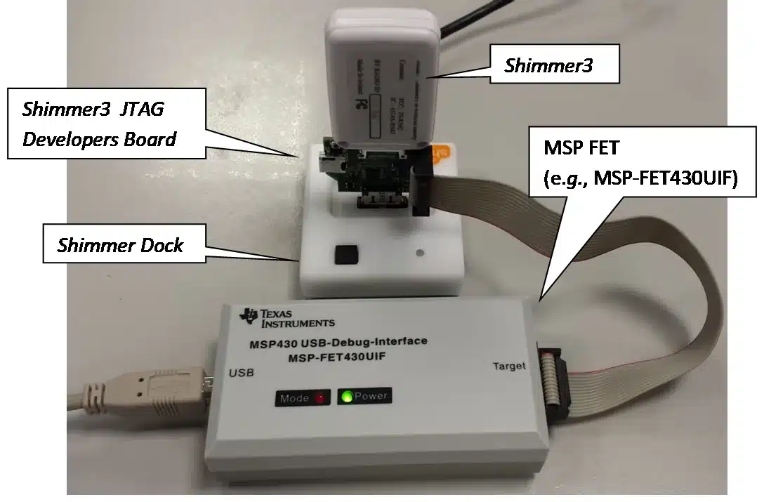
Figure 3‑1: Typical hardware configuration for programming and debugging of a Shimmer3.
4. Firmware Development
Getting the Shimmer3 firmware source, its toolchain and building it are described in Firmware Development in the Shimmer3/3R User Manual and in the README of https://github.com/ShimmerResearch/shimmer3-firmware.
For debugging over JTAG you also need a FET, such as the MSP-FET430UIF or an equivalent from Elpotronic or another manufacturer, connected through this board as described in Chapter 3. Code Composer Studio™ from Texas Instruments is recommended; any compiler and debugger that supports the MSP430F5437A can be used instead (e.g. IAR Embedded Workbench, Rowley CrossWorks, MSP430-GCC). A firmware image built as a TI-TXT flash image (.txt) can also be programmed without a FET, with Consensys and a Shimmer Dock (Programming a Shimmer).
5. Possible Prototyping Applications
When designing custom firmware for the Shimmer3, as would be the case in the applications discussed in this section, particular care must be taken to verify the configuration of any Shimmer3 pins in the Shimmer application code.
5.1. Connecting an Analog Output Sensor
Using the sensor specification, chose either the Shimmer3 + 3 V (PV_SHIMMER – JTAG pin 4) or another external source as the power supply connections to the sensor. The output of the sensor should be tied to either the A6, A7 or A15 ADC inputs as appropriate. If the sensor output is outside of the range of the Shimmer ADC (+ 3 V max) an attenuator must be added.
If the sensor uses the bipolar power supply, the output must be AC-coupled via a series capacitor to an appropriate DC bias resistor network connected to the ADC input pin.
Any unused GPIO pins can be used to configure control pins on the sensor. Verify the configuration of any of these pins in the Shimmer application code.
5.2. Connecting a Digital Output Sensor using the SPI interface
When using the Shimmer3 JTAG Developer Board with Shimmer3, the SPI bus is shared with the microSD, making the interface much more complicated than that for the PROTO3 Deluxe Expansion Board, which uses the dedicated internal bus. For that reason, Shimmer recommends use of PROTO3 Deluxe Expansion Board wherever possible. Furthermore, Shimmer recommends that the Shimmer3 JTAG Developer Board should not be used in cases where microSD is used, noting that this use case will receive only limited support from Shimmer.
If connecting a digital sensor to the Shimmer3 via the Shimmer3 JTAG Developer Board, attention must be given to the required master-slave relationship in your application (Shimmer is usually master). To create the digital interface, connect up the SPI SI,SO, and CLK pins with an additional GPIO pin as a Chip Select. The USART B1 module of the MSP430 will need to be configured for SPI mode– as is the default case in the SDLog stock firmware. For power supply connections, chose either the Shimmer3 on-board + 3 V or an external power supply connection to the sensor as appropriate. A level shift IC may be required if the sensor output voltages exceeds the Shimmer3 voltage supply level.
The application must ensure that the bus is correctly multiplexed using the SPI chip-select signals. Any remaining GPIO pins can be used to configure control pins on the sensor. Verify the configuration of any of these pins in the Shimmer application code.
5.3. Connecting to a Serial UART
Similar to the SPI directions above, the USART A0 module must be configured for UART operation. The output signals will be digital at a + 3 V reference. A level shifter IC or RS-232 level shifter may be used to interface with instrumentation or other computers.
5.4. Connecting a Parallel Bus interface
To use a parallel bus interface, most pins will need to be configured as GPIO instead of the default functionality. Up to an 11-pin bus can be configured.
5.5. Connecting an External Power Battery Pack
There are two options available if an external power supply is required. The first is to connect an external source via the on-board Mini-USB socket. In this case, the Shimmer3 JTAG Developer Board mode selection switch must be in the JTAG programming mode position. The Shimmer3 will think that it is in DEBUG mode and the respective JTAG pins on the JTAG header and breakout connectors will be in JTAG functionality mode (as described in Table 2‑1).
The second is to solder an external battery pack or power supply to the PV_PROG (J7-2) and GND (J7-1) breakout pins of the Shimmer3 JTAG Developer Board. In this case, it is recommended to isolate this power supply with a Schottky diode when the Shimmer battery is also in use. As before, if the voltage on PV_PROG is > 5.7 V, the Shimmer3 will think it is DEBUG mode and the JTAG pin functions will be activated. If it is < 5.7 V, the alternative pin functions (as listed in Table 2‑1) will be enabled.
Note: Both of these options will charge the Shimmer battery.
Note: Do not exceed 5.5 VDC on PV_PROG or 5 V on the USB V+ connection.
Note: Do not exceed 200 mA input.
Legal notices
Legal Notices and Disclaimer
Redistribution IS permitted provided that the following conditions are met:
Redistributions must retain the copyright notice, and the following disclaimer. Redistributions in electronic form must reproduce the above copyright notice, this list of conditions and the following disclaimer in the documentation and/or other materials provided with the document.
Neither the name of Shimmer Research Ltd. nor the names of its contributors may be used to endorse or promote products derived from this document without specific prior written permission.
THIS DOCUMENT IS PROVIDED BY THE COPYRIGHT HOLDERS AND CONTRIBUTORS “AS IS” AND ANY EXPRESS OR IMPLIED WARRANTIES, INCLUDING, BUT NOT LIMITED TO, THE IMPLIED WARRANTIES OF MERCHANTABILITY AND FITNESS FOR A PARTICULAR PURPOSE ARE DISCLAIMED. IN NO EVENT SHALL THE COPYRIGHT OWNER OR CONTRIBUTORS BE LIABLE FOR ANY DIRECT, INDIRECT, INCIDENTAL, SPECIAL, EXEMPLARY, OR CONSEQUENTIAL DAMAGES (INCLUDING, BUT NOT LIMITED TO, PROCUREMENT OF SUBSTITUTE GOODS OR SERVICES; LOSS OF USE, DATA, OR PROFITS; OR BUSINESS INTERRUPTION) HOWEVER CAUSED AND ON ANY THEORY OF LIABILITY, WHETHER IN CONTRACT, STRICT LIABILITY, OR TORT (INCLUDING NEGLIGENCE OR OTHERWISE) ARISING IN ANY WAY OUT OF THE USE OF THIS DOCUMENT, EVEN IF ADVISED OF THE POSSIBILITY OF SUCH DAMAGE.
