
1. Introduction
This reference is for firmware developers and for anyone testing or repairing a Shimmer3: the mainboard’s pin assignments, the Bluetooth radio, the microSD data path, the battery charger, and the conventions for the LEDs. Everything a user needs to operate a Shimmer is in the Shimmer3/3R User Manual.
Firmware development itself (the source, toolchains and building and programming images) is described in each firmware repository’s README and in the log-and-stream-common documentation; see Firmware Development in the Shimmer3/3R User Manual. The Shimmer3 JTAG Developer Board User Guide covers debugging over JTAG.
Shimmer3R: Section 2 covers both generations. The rest of this reference describes the Shimmer3 mainboard (MSP430F5437A); Shimmer3R has a different processor, radio and ADC, and the Shimmer3R hardware section of the Shimmer3/3R User Manual lists the differences.
2. Mainboard detail
Shimmer3R: Each section gives the Shimmer3 mainboard (MSP430F5437A) first, then the Shimmer3R (STM32U5A5). Shimmer3R has no internal expansion connector.
2.1. Connector Pin Assignments
Shimmer3 External Expansion Connector
Conn Pin |
Net Name |
Interruptible? |
Function |
J5-1 |
PV_CHG |
N |
Battery Charging Power 5-6VDC. Do not exceed 300mA connector current rating When >5.7V is applied to this pin, DEBUG mode is activated and JTAG signals are activated. JTAG signals are indicated in ()’s below. |
J5-2 |
SA_SOMI_RXD |
N |
USART A0: Serial |
J5-3 |
SA_SIMO_TXD |
N |
USART A0: Serial |
J5-4 |
FLASH_SCLK_EXT |
N |
USART B1: SPI (wired to microSD) |
J5-5 |
FLASH_SOMI |
N |
USART B1: SPI (wired to microSD) |
J5-6 |
FLASH_SIMO |
N |
USART B1: SPI (wired to microSD) |
J5-7 |
SBWTCK |
N |
BSL programming |
J5-8 |
MSP_RESET_N |
N |
BSL programming and Global Reset |
J5-9 |
DETECT_N (JTAG_TDI) |
N |
Card detect output signal to flash controller (JTAG TDI signal) |
J5-10 |
GPIO_EXTERNAL_RADIO_DD |
Y |
GPIO. Alternate function is reserved for coprocessor Bi-Spy Wire |
J5-11 |
BSL_RX_LED_BLU (JTAG_TMS) |
Y |
BSL programming, BLU LED SIGNAL (JTAG TMS signal) |
J5-12 |
ADC6_FLASHDAT2 |
N |
ADC input or GPO. Also used for SD mode flash access |
J5-13 |
ADC7_FLASHDAT1 |
N |
ADC input or GPO. Also used for SD mode flash access |
J5-14 |
BSL_TX_LED_GR1 (JTAG_TCK) |
Y |
BSL Programming, LED signal (JTAG_TCK signal) |
J5-15 |
FLASH_CS_N (JTAG_TDO) |
Y |
Flash CS or SD Mode DAT3 line (JTAG TDO Signal) |
J5-16 |
ADC15_RADIO_DC |
Y |
ADC Input. Alternate function is reserved for coprocessor Bi-Spy Wire |
J5-17 |
PV |
N |
Regulated Board power output: 3.0VDC @ 100ma* |
J5-18 |
GND |
N |
Board Ground |
J5-TABS/SHELL |
GND |
N |
Board Ground |
* Exact current capacity will vary based on operating state of integrated peripherals and processor.
Shimmer3 Internal Expansion Connectors
For function descriptions see previous table.
Conn and Pin Number |
Net Name |
Conn and Pin Number |
Net Name |
J6-1 J6-20 |
PV |
J7-1 J7-2 J7-19 J7-20 |
PV_REG |
J6-2 J6-19 |
GPIO_INTERNAL2 |
||
J6-3 J6-18 |
GPIO_INTERNAL |
J7-3 J7-18 |
ADC1 |
J6-4 J6-17 |
SA_SIMO_TXD |
J7-4 J7-17 |
ADC12 |
J6-5 J6-16 |
SA_SOMI_RXD |
J7-5 J7-16 |
ADC13 |
J6-6 J6-15 |
SA_SCLK |
J7-6 J7-15 |
ADC14 |
J6-7 J6-14 |
SB_SCL |
J7-7 J7-14 |
GPIO_INTERNAL1 |
J6-8 J6-13 |
SB_SDA |
J7-8 J7-13 |
EXP_RESET_N |
J6-9 J6,10 J6-11 J6-12 |
GND |
J7-9 J7,10 J7-11 J7-12 |
GND |
J6-TABS |
GND |
J7-TABS |
GND |
Shimmer3R External Connector
The Shimmer3R external (dock) connector, J5, is the same 18-way ST60-18P connector as on Shimmer3, so a Shimmer3R fits the same docks, but most of its contacts carry different signals. The microSD card lines are switched between the processor and the dock: while docked, the card is on the dock’s contacts (marked SD card), and the processor has no access to it. The source is the Shimmer3R schematic (SR38-PCBA-004, sheet 5).
| Pin | Net name | Function |
|---|---|---|
| 1 | PV_CHG | Charge input from the dock (also used to detect docking) |
| 2 | DOCK_RXD | Dock UART, into the Shimmer3R |
| 3 | DOCK_TXD | Dock UART, out of the Shimmer3R |
| 4 | FLASH_SCLK_EXT | SD card clock, while docked |
| 5 | FLASH_SOMI_EXT | SD card data 0, while docked |
| 6 | FLASH_SIMO_EXT | SD card command, while docked |
| 7 | BOOT0 | Processor boot mode: the dock selects the system bootloader for programming |
| 8 | NRST | Processor reset |
| 9 | DETECT_N | Output from the processor (PC5) |
| 10 | GPIO_EXTERNAL | General purpose I/O (processor pin PE9) |
| 11 | BSL_RX | System bootloader UART, into the Shimmer3R (processor pin PA3) |
| 12 | GPIO_ADC_EXT_EXP1 | Analogue input Ext A1; SD card data 2 while docked |
| 13 | GPIO_ADC_EXT_EXP0 | Analogue input Ext A0; SD card data 1 while docked |
| 14 | BSL_TX | System bootloader UART, out of the Shimmer3R (processor pin PA2) |
| 15 | FLASH_DAT3_EXT | SD card data 3, while docked |
| 16 | GPIO_ADC_EXT_EXP2 | Analogue input Ext A2 |
| 17 | PV_3.0V | +3.0 V regulated supply |
| 18 | GND | Ground |
| 19–24 | GND | Mounting pads and tabs |
Table 2‑1R Shimmer3R External Connector Pin Assignment
Shimmer3R has no internal expansion connector.
2.2. CPU Pin Assignment
Shimmer3
The CPU pin connections for Shimmer developers are listed below:
| Pin Name | Pin # | Board Name | Use | ** Type** |
| DVCC | 16,51,31,67 | PV_MSP | Power | Analogue |
| AVCC | 11 | PV_MSP | Power | Analogue |
| VREF | 9 | PV_VREF_MSP | A/D Ref | Analogue |
| VREFN | 10 | GND | A/D Ref | Analogue |
| DVSS | 15,50,30,68 | GND | Power | Analogue |
| AVSS | 12 | GND | Power | Analogue |
| VCORE | 11 | PV_MSPC | Power | Analogue |
| TEST | 71 | SBWTCK | BSL, SBW | Input |
| TCK | 75 | JTAG_TCK | JTAG | Input |
| TMS | 74 | TP_JTAG_TMS | JTAG | |
| TDI | 73 | TP_JTAG_TDI | JTAG | |
| TDO | 72 | TP_JTAG_TDO | JTAG | |
| RST_N | 76 | MSP_RESET_N | BSL, SBW, JTAG | Open Drain |
| XIN | 13 | CLK_MSP_XIN | Primary XTAL | Clocking |
| XOUT | 14 | CLK_MSP_XOUT | Primary XTAL | Clocking |
| XT2IN | 69 | CLK_MSP_HF_XIN | 8MHz Resonator | Clocking |
| XT2OUT | 70 | CLK_MSP_HF_XOUT | 8MHz Resonator | Clocking |
| P1.0 | 17 | RADIO_STATUS | RADIO, RADIO EXP | Input (IRQ) |
| P1.1 | 18 | BSL_TX_LED_GR1 | BSL/LED | Output |
| P1.2 | 19 | BSL_RX_LED_BLU | BSL/LED | |
| P1.3 | 20 | RADIO_RTS | RADIO | INPUT(IRQ) |
| P1.4 | 21 | GPIO_INTERNAL | TBD | Input (IRQ) |
| P1.5 | 22 | GPIO_EXTERNAL_RADIO_DD | TBD, RADIO EXP | Input (IRQ) |
| P1.6 | 23 | USER_N | User Button | Input (IRQ) |
| P1.7 | 24 | MPU_INT | Kinematics | Input(IRQ) |
| P2.0 | 25 | GPIO_EXTERNAL1 | Expansion | Input (IRQ) |
| P2.1 | 26 | GPIO_EXTERNAL2 | Expansion | Input (IRQ) |
| P2.2 | 27 | RADIO_CTS | RADIO | Input (IRQ) |
| P2.3 | 28 | DOCK | Input (IRQ) | |
| P2.4 | 29 | MAG_DRDY | Kinematics | Input (IRQ) |
| P2.5 | 32 | MAG_INT1 | Kinematics | Input (IRQ) |
| P2.6 | 33 | CHG_STAT1 | CHARGER | Input (IRQ) |
| P2.7 | 34 | CHG_STAT2 | CHARGER | Input (IRQ) |
| P3.0 | 35 | SA_SCLK_R | Expansion | Output |
| P3.1 | 36 | SB_SDA | USART B0 | Output |
| P3.2 | 37 | SB_SCL | USART B0 | Input |
| P3.3 | 38 | EXP_RESET_N | Expansion | Output |
| P3.4 | 39 | SA_SIMO_TXD | USART A0 | Output |
| P3.5 | 40 | SA_SOMI_RXD | USART A0 | Input |
| P3.6 | 41 | RADIO_SCLK_R | RADIO EXP, USART A1 | Output |
| P3.7 | 42 | FLASH_SIMO | FLASH, USART B1 | Output |
| P4.0 | 43 | FLASH_CS_N_FLASH_DAT3 | FLASH | Output |
| P4.1 | 44 | SD_DETECT_N | FLASH | Input |
| P4.2 | 45 | SW_FLASH | FLASH | Output |
| P4.3 | 46 | SW_BT | RADIO | Output |
| P4.4 | 47 | BT_RESET_N | RADIO | Output |
| P4.5 | 48 | BT_FACTORY | RADIO | Output |
| P4.6 | 52 | SW_TCXO | TCXO | Output |
| P4.7 | 53 | TCXO_CLK_R | TCXO | Input (Clock) |
| P5.4 | 54 | FLASH_SOMI | FLASH | Input |
| P5.5 | 55 | FLASH_SCLK_R | FLASH | Output |
| P5.6 | 56 | RADIO_TXD_SIMO | RADIO, RADIO EXP | Output |
| P5.7 | 57 | RADIO_RXD_SOMI | RADIO, RADIO EXP | Input |
| P7.2 | 58 | LED_RD | LED | Output |
| P7.3 | 59 | LED_GR | LED | Output |
| P8.0 | 60 | LED_YE | LED | Output |
| P8.1 | 61 | RADIO_CS_N | RADIO EXP | Output |
| P8.2 | 62 | RADIO_RESET_N | RADIO EXP | Output |
| P8.3 | 63 | SW_RADIO | RADIO EXP | Output |
| P8.4 | 64 | NOT ROUTED | ||
| P8.5 | 65 | NOT ROUTED | ||
| P8.6 | 66 | SW_ACCCEL | Kinematics | Output |
| P6.0 | 77 | DETECT_N | FLASH | Output |
| P6.1 | 78 | SEL_ADC | Expansion | Output |
| P6.2 | 79 | BATTERY | ADC | Analogue Input |
| P6.3 | 80 | ACCEL_X | Low Noise Accel | Analogue Input |
| P6.4 | 1 | ACCEL_Y | Low Noise Accel | Analogue Input |
| P6.5 | 2 | ACCEL_Z | Low Noise Accel | Analogue Input |
| P6.6 | 3 | ADC6_FLASHDAT2 | Ext GPIO, ADC | Analogue Input |
| P6.7 | 4 | ADC7_FLASHDAT1 | Ext GPIO, ADC | Analogue Input |
| P7.4 | 5 | ADC12 | ADC | Analogue Input |
| P7.5 | 6 | ADC13 | ADC | Analogue Input |
| P7.6 | 7 | ADC14 | ADC | Analogue Input |
| P7.7 | 8 | ADC15_RADIO_DC | ADC, RADIO EXP | Analogue Input |
Table 2‑3 Shimmer3 CPU pin assignment
Shimmer3R
The Shimmer3R processor is an STM32U5A5QJ (UFBGA132 package). The table lists every pin its firmware assigns, by port pin; the source is the firmware’s STM32CubeIDE project (LogAndStream_Shimmer3R_UBGA132_SMPS.ioc), and the Shimmer3R peripheral allocation in the firmware documentation explains which bus serves which part. Pins not listed are unassigned.
| Pin | Board name | Function | Use |
|---|---|---|---|
| PA0 | LED_UPR_RD | TIM2_CH1 | Upper LED, red (PWM) |
| PA1 | DOCK_DETECT | GPIO, interrupt | Dock detect |
| PA2 | BSL_TX | USART2_TX | System bootloader UART (not used by the application) |
| PA3 | BSL_RX | USART2_RX | System bootloader UART (not used by the application) |
| PA6 | USER_BTN | GPIO, interrupt | User button |
| PA8 | SW_MIC | GPIO output | Microphone supply switch |
| PA9 | USB_VBUS | GPIO input, interrupt | USB power detect |
| PA10 | CS_HIGH_G | GPIO output | High-g accelerometer (ADXL371) chip select, SPI1 |
| PA11 | — | USB_OTG_HS_DM | USB data − |
| PA12 | — | USB_OTG_HS_DP | USB data + |
| PA13 | — | SWDIO | Debug (SWD) |
| PA14 | — | SWCLK | Debug (SWD) |
| PA4 | GPIO_INTERNAL6 | GPIO | Expansion |
| PB1 | GPIO_INTERNAL3 | GPIO | Expansion |
| PB2 | GPIO_INTERNAL4 | GPIO input | Expansion |
| PB3 | — | SWO | Debug (trace output) |
| PB4 | — | SPI3_MISO | ExG bus (ADS1292R) |
| PB5 | — | SPI3_MOSI | ExG bus (ADS1292R) |
| PB6 | DOCK_TXD | USART1_TX | Dock UART |
| PB7 | DOCK_RXD | USART1_RX | Dock UART |
| PB8 | — | I2C1_SCL | Sensor I2C bus: magnetometer (LIS2MDL), EEPROM |
| PB9 | — | I2C1_SDA | Sensor I2C bus |
| PB10 | LED_UPR_GR | TIM2_CH3 | Upper LED, green (PWM) |
| PB11 | LED_UPR_BLU | TIM2_CH4 | Upper LED, blue (PWM) |
| PB12 | LIS2DW12_INT1 | GPIO, interrupt | Wide-range accelerometer interrupt |
| PB13 | — | SPI2_SCK | Sensor SPI bus 2: wide-range accelerometer (LIS2DW12) |
| PB14 | — | SPI2_MISO | Sensor SPI bus 2 |
| PB15 | — | SPI2_MOSI | Sensor SPI bus 2 |
| PC0 | CS_ADS7028 | GPIO output | External ADC (ADS7028) chip select, SPI1; it carries every sensor analogue channel |
| PC2 | CS_LSM6DSV | GPIO output | Low-noise accelerometer and gyroscope (LSM6DSV) chip select, SPI1 |
| PC3 | VBAT_SENSE | ADC1_IN4 / ADC2_IN4 | Battery voltage |
| PC4 | SW_SD_MCU_DOCK | GPIO output | microSD card switch: processor or dock |
| PC5 | DETECT_N | GPIO output | |
| PC6 | BT_CP_ROLE | GPIO | Bluetooth module |
| PC7 | SW_BT | GPIO output | Bluetooth supply switch |
| PC8–PC11 | SDMMC1_D0–D3 | SDMMC1 | microSD card, 4-bit data |
| PC12 | SDMMC1_CK | SDMMC1 | microSD card clock |
| PC13 | GPIO_INTERNAL0 | GPIO, interrupt | Expansion |
| PC14, PC15 | — | OSC32_IN, OSC32_OUT | 32.768 kHz crystal |
| PD0 | SD_DETECT_N | GPIO input, interrupt | microSD card detect |
| PD1 | SW_FLASH | GPIO output | |
| PD2 | SDMMC1_CMD | SDMMC1 | microSD card command |
| PD3 | SW_SENSE | GPIO output | Sensor supply switch |
| PD4 | GPIO_INTERNAL1 | GPIO, interrupt | Expansion |
| PD5 | GPIO_INTERNAL2 | GPIO | Expansion |
| PD6 | CS_BMP390 | GPIO output | Pressure sensor chip select, SPI1 |
| PD7 | CS_LIS2DW12 | GPIO output | Wide-range accelerometer chip select, SPI2 |
| PD8 | BT_TXD | USART3_TX | Bluetooth UART |
| PD9 | BT_RXD | USART3_RX | Bluetooth UART |
| PD10 | BT_LP_MODE | GPIO | Bluetooth module |
| PD11 | BT_CTS | USART3_CTS | Bluetooth UART flow control |
| PD12 | BT_RTS | USART3_RTS | Bluetooth UART flow control |
| PD13 | BT_RST | GPIO | Bluetooth module reset |
| PD14 | BT_CONNECTION | GPIO, interrupt | Bluetooth connection status |
| PD15 | BT_CYSPP | GPIO, interrupt | Bluetooth module |
| PE0 | GPIO_INTERNAL5 | GPIO input | Expansion |
| PE2, PE6 | — | Reserved | |
| PE3 | LED_LWR_RD | TIM3_CH1 | Lower LED, red (PWM) |
| PE4 | LED_LWR_GR | TIM3_CH2 | Lower LED, green (PWM) |
| PE5 | LED_LWR_BLU | TIM3_CH3 | Lower LED, blue (PWM) |
| PE7 | LSM6DSV_INT1 | GPIO, interrupt | Low-noise accelerometer and gyroscope interrupt |
| PE8 | BT_HOST_WAKE | GPIO | Bluetooth module |
| PE9 | GPIO_EXTERNAL | GPIO | Expansion (shares interrupt line 9 with PA9, so it cannot be an interrupt input) |
| PE10 | LIS2MDL_DRDY | GPIO, interrupt | Magnetometer data ready |
| PE11 | BMP390_INT | GPIO, interrupt | Pressure sensor interrupt |
| PE12 | SW_SENSE_IO | GPIO output | |
| PE13 | — | SPI1_SCK | Sensor SPI bus 1: external ADC, low-noise accelerometer and gyroscope, pressure, high-g accelerometer |
| PE14 | — | SPI1_MISO | Sensor SPI bus 1 |
| PE15 | — | SPI1_MOSI | Sensor SPI bus 1 |
| PF0 | CHG_STAT1 | GPIO input | Battery charger status |
| PF1 | CHG_STAT2 | GPIO input | Battery charger status |
| PF3 | MIC_CK | ADF1_CCK0 | Microphone (PDM) clock |
| PF4 | MIC_SD | ADF1_SDI0 | Microphone (PDM) data |
| PF14 | — | I2C4_SCL | Expansion I2C bus; production test |
| PF15 | — | I2C4_SDA | Expansion I2C bus; production test |
| PG9 | — | SPI3_SCK | ExG bus (ADS1292R) |
| PH0, PH1 | — | OSC_IN, OSC_OUT | High-speed crystal |
| PH3 | — | BOOT0 | Boot mode |
Table 2‑3R Shimmer3R CPU pin assignment
2.3. Block diagram
Shimmer3 only. Figure 2‑1 presents a block diagram of the Shimmer3 mainboard with core components and interconnections between integrated devices illustrated.
The central element of the platform is the low-power MSP430F5437A microprocessor which controls the operation of the device. Nearly every feature of the CPU is exercised in the Shimmer implementation. The CPU configures and controls various integrated peripherals through I/O pins, some of which are available on the internal/external-expansion connectors. The CPU has an integrated 16-channel 12bit analogue-to-digital converter (ADC) which is used to capture sensor data from the low noise accelerometer, battery, or sensor expansions, such as GSR, Bridge Amp and Proto 3 Deluxe. The external expansion also allows communication to and from the mainboard using the docking station.
The Shimmer board has a built in microSD Flash socket for additional storage and has five light-emitting diodes (LED) for display purposes. It also has an on-off switch and a software-defined user button. For wireless data streaming, the platform is equipped with a Bluetooth radio module and has the capacity for an additional alternative radio.
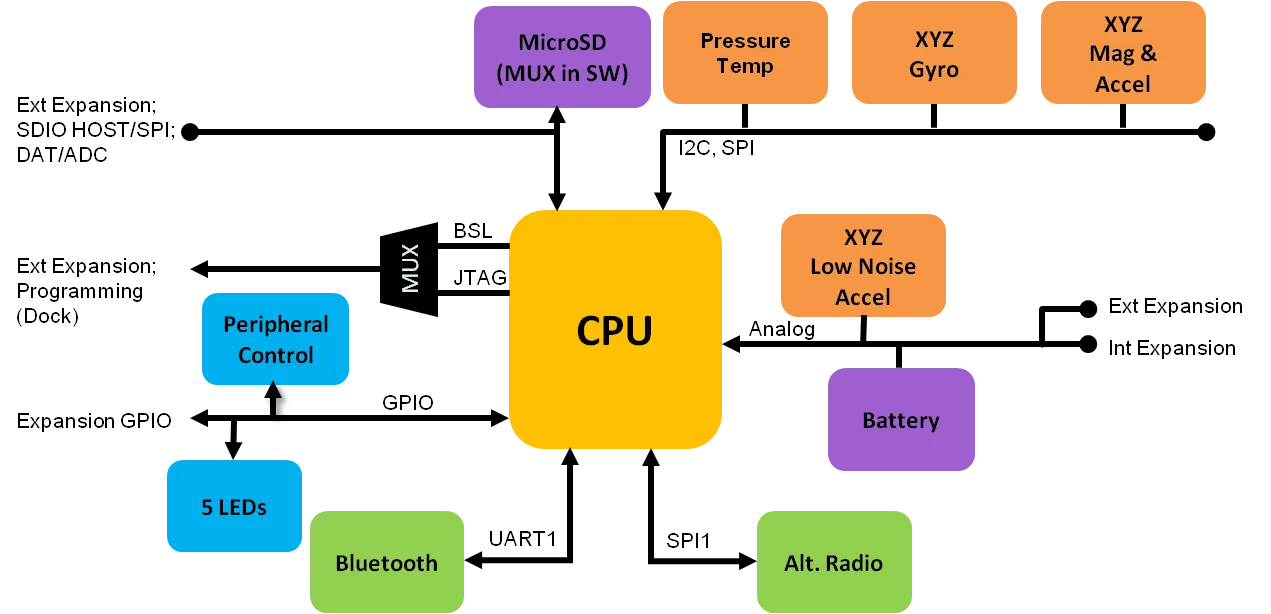
Figure 2‑1 Shimmer3 Core Component Block Diagram
2.4. Power switching and the regulator
Shimmer3 only. A sliding switch is used to control board power states.
Soft power switching is provided for the Bluetooth radio module, temperature compensated crystal oscillator, FFC expansion (Radio Peripheral) and microSD socket (see microSD host data bypass for microSD card power control). Other modules have integrated shutdown functionality.
Shimmer’s on-board regulator can provide 100mA continuous current and tolerates surges until a thermal limit is reached. Expansion devices must be current limited or have independent regulation running off the PV_REG expansion pin. Exceeding the 100mA limit of the regulator, whilst possible, is not recommended without detailed analysis and qualification of both electrical and thermal design margin.
3. Bluetooth radio
One of the key functions of the Shimmer board is its ability to communicate as a wireless platform. Shimmer uses a Bluetooth Radio module.
3.1. Bluetooth (IEEE 802.15.1)
Bluetooth is a low-cost, low-power, robust, short-range wireless communication protocol which was initially founded by Ericsson in 1994 to replace traditional mobile phone and computer cables with wireless links. It operates in the license free 2.4 GHz ISM (industrial, scientific, medical) band with a short range (power-class-dependent: 1 metre, 10 metres, 100 metres) transceiver in each device. With the introduction of the (EDR) Enhanced Data Rate feature [1], devices can communicate with each other at up to 3Mbps. The Bluetooth special interest group (SIG) was founded in 1998 by companies such as Ericsson, Nokia and Intel and the core system consists of an RF transceiver, baseband and protocol stack. Bluetooth radios are designed for busy environments with many users. Up to eight Bluetooth devices can communicate together in a network called a piconet. The piconet is a point to multipoint network consisting of one master and up to seven slave devices. Multiple piconets can coexist and join together to form scatternets. Bluetooth uses 79 1MHz channels to transmit data. Interference between other ISM band devices (802.11 and 802.15.4 devices) and other Bluetooth piconets is minimised using frequency hopping spread spectrum (FHSS), where the carrier is rapidly switched (hops) among the 79 available channels. The frequency hopping sequence is controlled by the master within the piconet. Other Bluetooth interference reduction techniques include adaptive power control, Channel Quality Driven Data Rate (CQDDR) and Adaptive Frequency Hopping (AFH) [2]. Extensive documentation and analysis of Bluetooth and its applications can be accessed from the Bluetooth SIGs website at www.bluetooth.com.
3.2. The Bluetooth module
Early Shimmer3 units use the Roving Networks RN-42 [3] Class 2 Bluetooth module to communicate via an integrated 2.4GHz antenna. This module was found to be well engineered and very configurable [4], reliable and robust. This module contains a full Version 2 Bluetooth Protocol Stack and supports the Serial Port Profile which facilitates rapid application development. The Bluetooth module is connected to the MSP430 directly via the USART1 serial connection. It can also be controlled by ASCII strings over the Bluetooth RF link. The RN-42 has a range of more than 10 metres (33 feet) and the transmitted power can be adjusted depending on the application distance. The system has seventy-nine channels with channel intervals of 1MHz and offers a robust secure link via frequency hopping spread spectrum (FHSS) and error correction schemes. Users can expect to communicate with the Shimmer USART at speeds up to 230kbaud, with 115kbaud as the default and recommended value.
Later Shimmer3 units carry the Microchip RN4678, a dual-mode module that adds Bluetooth Low Energy to the same Serial Port Profile connection. Which radio and firmware a unit has is reported to Consensys.
4. microSD host data bypass
To improve usability, Shimmer incorporates a wide bandwidth analogue MUX and tri-state logic buffering on certain signals routed to the external connector to provide direct and immediate access to flash memory using an external SD-flash card controller (SDHOST) for high-speed data transfer. Shimmer Applications that use the microSD card will require firmware that allows for the SD specification’s requirement of a power-cycle to change from SPI mode (the card talking to the MSP430) back to SDIO mode (the card is controlled by the USB flash media controller). Power-cycling the card requires explicit control of the card’s interface pins, setting them to LOW (zero Volts).
The Host Data Bypass implementation has been simplified when compared to prior generation sensor platforms. When a firmware application detects that the Shimmer is docked, it can complete pending activities, power cycle the flash media (including lowering all SPI pins going to the media), reconfigure the data path and the assert a media-detect signal to the host computer via a USB flash media controller peripheral.
Always use a Shimmer Dock v3 (or higher) for best performance.
Earlier docks required a logic timing-critical scheme, which has been deprecated.
5. Battery charger
The Shimmer uses a diode wired-OR to prevent device damage from reversed battery leads and allow operation from external power while charging.
The Texas Instruments LM3658D Smart Li Charger is used for battery management. The LM3658D implements a multi-phase charge profile including battery conditioning and overcharge protection. The default Rset resistor value of 22.1kΩ provides conservative 125mA charge limiting. The supplied battery pack (400 mAh on current Shimmer3 units, 450 mAh on earlier units) includes secondary failsafe protection against over/under voltage and over-discharge – all user-selected or installed batteries must provide secondary failsafe protection. The maximum discharge current on the supplied battery is 3.360A, a rate far exceeding expected conditions for sensing applications.
6. LED colour conventions
The lower LED location is tri-coloured (green, yellow and red) and is meant for operational status; the upper location is bi-coloured (blue and green) and is meant for the data communication mode. Firmware developers are encouraged to follow international conventions for indicator lights, as LogAndStream does:
- Operational status: green for correct operation, yellow for a warning, red for an error.
- Data status: blue for Bluetooth, green for sensing.
The user button gives no tactile feedback, so firmware should show a press on an LED; LogAndStream lights the lower LED green while the button is held. The LED feedback reference describes how LogAndStream drives each LED.
7. References
[1] Bluetooth Special Interest Group, Serial port Profile Specification, Vol. 7 Part B of the Bluetooth Specification Version 2, November, 2004.
[2] C. Hodgdon, Adaptive frequency hopping for reduced interference between Bluetooth and wireless LAN, Ericsson Technology Licensing, May 2003.
[3] Roving Networks, Bluetooth Module RN-42, Available at http://www.rovingnetworks.com
[4] Roving Networks, Bluetooth Module RN-46 Command Set, Available at http://www.rovingnetworks.com
Legal Notices and Disclaimers
Legal Notices and Disclaimers
Disclaimers
SHIMMER RESEARCH LTD. MAKES NO WARRANTY OF ANY KIND WITH REGARD TO THIS MATERIAL, INCLUDING, BUT NOT LIMITED TO, THE IMPLIED WARRANTIES OF MERCHANTABILITY AND FITNESS FOR A PARTICULAR PURPOSE. SHIMMER RESEARCH LTD. ASSUMES NO RESPONSIBILITY FOR ANY ERRORS THAT MAY APPEAR IN THIS DOCUMENT. SHIMMER RESEARCH LTD. MAKES NO COMMITMENT TO UPDATE NOR TO KEEP CURRENT THE INFORMATION CONTAINED IN THIS DOCUMENT.
THIS SPECIFICATION IS COPYRIGHTED BY AND SHALL REMAIN THE PROPERTY OF SHIMMER RESEARCH LTD. NO LICENSE, EXPRESS OR IMPLIED, BY ESTOPPEL OR OTHERWISE TO ANY INTELLECTUAL PROPERTY RIGHTS IS GRANTED HEREIN.
SHIMMER RESEARCH LTD. DISCLAIMS ALL LIABILITY, INCLUDING LIABILITY FOR INFRINGEMENT OF ANY PROPRIETARY RIGHTS, RELATING TO USE OF THE MATERIALS AND IMPLEMENTATION OF INFORMATION IN THIS SPECIFICATION. SHIMMER RESEARCH LTD. DOES NOT WARRANT OR REPRESENT THAT SUCH USE OR IMPLEMENTATIONS WILL NOT INFRINGE SUCH RIGHTS.
Redistribution IS permitted provided that the following conditions are met:
Redistributions must retain the copyright notice, and the following disclaimer. Redistributions in electronic form must reproduce the above copyright notice, this list of conditions and the following disclaimer in the documentation and/or other materials provided with the document.
Neither the name of Shimmer Research Ltd. nor the names of its contributors may be used to endorse or promote products derived from this document without specific prior written permission.
SHIMMER RESEARCH LTD. RETAINS THE RIGHT TO MAKE CHANGES TO THESE SPECIFICATIONS AT ANY TIME, WITHOUT NOTICE.
CAUTION
RISK OF EXPLOSION IF BATTERY IS REPLACED BY AN INCORRECT TYPE.
DISPOSE OF USED BATTERIES ACCORDING TO THE INSTRUCTIONS.
Legal Notices
Shimmer Research Ltd. software products are copyrighted by and shall remain the property of Shimmer Research Ltd. Use, duplication or disclosure is subject to restrictions stated in the three clause BSD license, or in the case of software delivered to the government, in accordance with the software license agreement as defined in FAR 52.227-7013.The Shimmer logo is a registered trademark of Shimmer Research Ltd.

Other brands, marks and names mentioned herein may be the property of their respective owners and used in accordance with published guidelines.
© SHIMMER RESEARCH LTD., All Rights Reserved
