
1. Introduction
This document is an accompaniment to the Shimmer3 Bridge Amplifier+ Unit from Shimmer – called “BA+ Unit” in the remainder of this document*.* Its purpose is to aid the user in getting started with the BA+ Unit.
The BA+ Unit contains a bridge amplifier, excitation source, and connector enabling force measurement with Shimmer. The unit is ideal for all load, weight, force, torque, and pressure measurements through the connection of a user-supplied strain gauge based bridge sensor or load cell. One application area is muscle capacity testing including pinch-grip, lift-bar, and grip-strength.
The Bridge Amplifier circuitry detects variance in resistance values when force is applied to the load cell. The small, lightweight, wearable form factor allows for measurements free from wired constraints to allow for natural range of motion, and measurement outside of a dedicated lab setting.
Additionally, the board has a connector and amplifier for Resistance measurement. For example, this can be used to measure data from a temperature sensor, like the Philips 21091A, or other resistance-based sensors with a range of 1kΩ – 20kΩ.
2. General Information
2.1. Pre-Requisites
A Shimmer3 Bridge Amplifier+ Unit programmed with appropriate firmware.
LogAndStream, which streams data over Bluetooth and logs it to the SD card. Shimmer units are shipped with it, and Consensys installs updates.
LogAndStream (v0.2.0 or greater) can be used to simultaneously log data to SD card and stream data over Bluetooth.
Firmware images are available for download from www.shimmersensing.com.
A suitable strain gauge load cell or resistance-based sensor.
2.2. Bridge Amplifier+ Unit Specification
Bridge Amplifier:
Gain1: 183.7 ± 1% (Normal Channel), 551 (3x Normal) ± 1% (High Gain Channel)
Frequency Range1: DC..1kHz (Normal Channel), DC..100Hz (High Gain Channel)
Common Mode Rejection1: higher than 110dB
Input Impedance1: 50MOhm
Input Signal Range: ±7mV, ±2.5mV/V (Normal Channel), 0-4mV, ±1.43mV/V (High Gain Channel)
Zero-load Noise: 12mV RMS both outputs, < 1% full-scale (Normal Channel), < 0.5% full-scale (High Gain Channel)
Excitation Voltage2: 2.8V ± 5%
Input Protection: Current limiting, EMI/RF suppression
Resistance Amplifier
Gain1: 10.1 +/-2%
Pull-up/Input Impedance: 200kOhms to +3.0V
Frequency Range1: DC..408Hz (2nd Order)
Signal Range: 280mV or 20kOhms (1kΩ-20kΩ measurement range recommended)
Zero-load Noise: 0.1 mV RMS at output.
Connections: Two 3.5mm jacks (headphone type) for 4 conductor shielded cable for Bridge Amplifier and Resistance Amplifier,
Current Consumption: < 100µA (Excitation disabled), 17mA (Excitation enabled3)
EEPROM memory: 2048 bytes.
3. Hardware Considerations
3.1. Board Layout
Note: For Shimmer3 Bridge Amplifier+ hardware purchased prior to January 2016, refer to section 8.1.
The figures in this section show the board layout for the BA+ Unit, with components labelled. The
area on the board within with the orange dashed lines is the part of the circuitry of the BA+ Unit
that is described in this User Guide. The area on the board outside of the orange dashed lines is the
circuitry of the Shimmer3, described in the Shimmer User Manual.
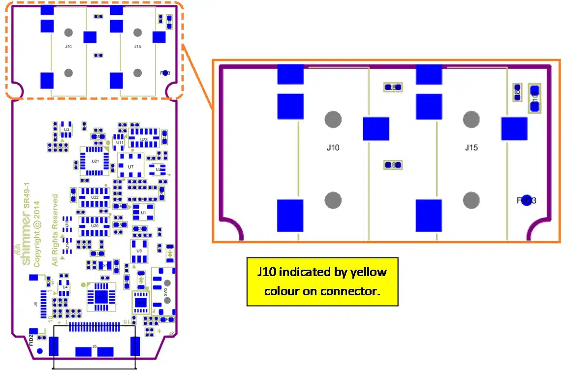
Figure 3‑1: BA+ Board Layout (bottom view)
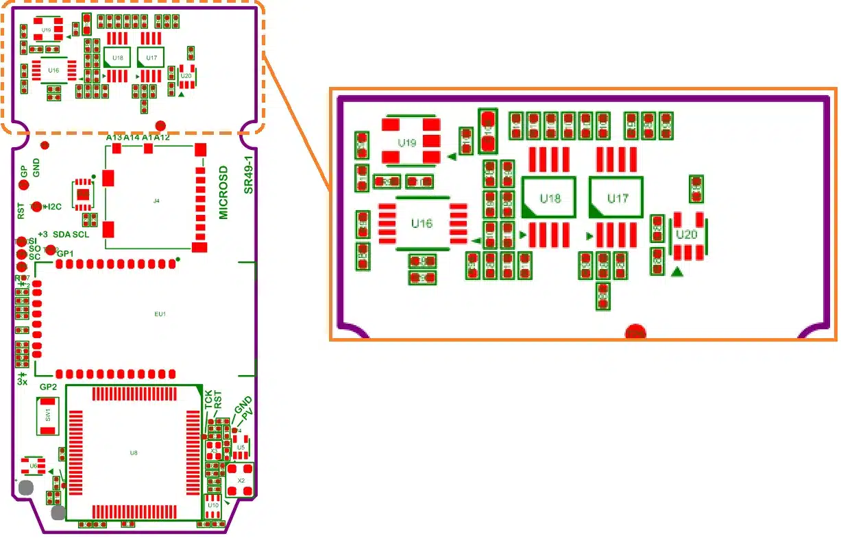
Figure 3‑2: BA+ Board Layout (top view)
3.2. Connections
The 3.5mm 4-position jack connectors, J10 and J15, (indicated in Figure 3‑1) have four connections each, as labelled in Error! Reference source not found.. Their connections are listed in the corresponding tables in this section.
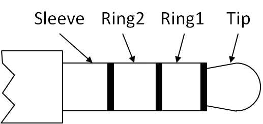
Figure 3‑3 Connector labels for 3.5mm 4-position jack
| Connector Pin# | Shimmer3 Label | Function / Notes |
|---|---|---|
| Sleeve (J15.1) | GND | Ground Connection |
| Tip (J15.2) | SGP | Signal (Positive) |
| Ring1 (J15.3) | SGN | Signal (Negative) |
| Ring2 (J15.4) | PV_SG | 2.8V if GPIO_INTERNAL1 is high. |
Table 3‑1 Shimmer Bridge Amplifier+ Expansion Board connections for J15.
Important Note: Do not insert a two-position 3.5mm plug into the J3 connector as this may cause a short-circuit between PV and GND.
| Connector Pin# | Shimmer3 Label | Function / Notes |
|---|---|---|
| Sleeve (J10.1) | GND | Ground Connection |
| Tip (J10.2) | SGN | RDIV1 (Signal) |
| Ring1 (J10.3) | GND | Ground Connection |
| Ring2 (J10.4) | GND | Ground Connection |
Table 3‑2 Shimmer Bridge Amplifier+ Expansion Board connections for J10.
Important Note: The pin-out of the J10 connector is not the same as that for other Shimmer3 expansions and is not compatible with Shimmer accessories, such as the Optical Pulse Sensing Probe.
A high quality four-position 3.5mm jack with cable is available for purchase from Shimmer. You can wire this connector to your load cell according to the connections in Error! Reference source not found..
3.3. Output Signals
Table 3‑3 below lists the ADC channel of the Shimmer3 to which each of the output signals from the Bridge Amplifier+ Expansion Board is connected.
| Signal | ADC channel | Function |
|---|---|---|
| Bridge Amplifier Low Gain | A14 | bipolar pre-amplification |
| Bridge Amplifier High Gain | A13 | additional 3x gain for unipolar load cells |
| Resistance Amplifier Output | A1 | resistance pre-amplification |
Table 3‑3 ADC channels for Bridge Amplifier+ Expansion Board output signals
4. Using the Bridge Amplifier+ Unit
4.1. Load Cell Calibration: Calculating Load
To convert the output of the Shimmer to a quantifiable unit you require:
Output specification for the load cell device you are using in mV/V.
Knowledge of the daughter board gain (Normal or High Gain Channel, see specification overview above).
The calculation procedure is:
Measure the ADC output difference (ADCDIFF) between a zero-load reading and the reading of interest in your application. Referencing the actual zero-load reading obviates consideration of DC offset error.
Convert the ADCDIFF into an analogue voltage difference (VDIFF) in mV using a ratio
3000mV / 4095bits = VDIFF (mV)/ ADCDIFF (bits)
where 4095 is the resolution of the Shimmer 12bit ADC
VDIFF (mV) / = ADCDIFF (bits) * 3000 mV/4095 bits
3. Divide the voltage by (2.8V x gain) to compute the load-cell output (LCOUT) in mV/V
LCOUT (mV/V) = VDIFF (mV) / (2.8V * gain)
4. Refer to the load cell calibration report or datasheet to determine the rated output (ROUT) in (mV/V)/lb or (mV/V)/kg.
LOAD = LCOUT / ROUT
Example Calculation:
The high gain output has a zero-output ADC value of 230. In a grip test using a Futek LMD500 the peak ADC value is 1430. What is the load in lbs?
ADCDIFF = 1430 bits – 230 bits = 1200 bits
VDIFF = 1200 bits * 3000 mV/4095 bits = 879 mV
LCOUT = 879 mV / (2.8V * 551) = 0.570 mV/V
This calibration data for the LMD500 used has a rated output of 2.83mV/V @ 300lbs.
LOAD = 0.570 (mV/V) / (2.83(mV/V) / 300lbs) = 60.42lbs
4.2. Resistance Calibration: Calculating Resistance
For the Resistance amplifier channel, the relationship between the resistance at the input, , and the voltage output, , is as follows:
where = 3V and should be measured in volts.
5. Firmware Considerations
Note: This section is only of concern to persons wishing to modify the firmware.
Users with firmware development experience who wish to develop custom firmware for the Bridge Amplifier+ Unit should follow the LogAndStream firmware, whose source is at https://github.com/ShimmerResearch/shimmer3-firmware.
Users should note that the excitation voltage for the load cell connection is enabled via GPIO_INTERNAL1. The amplifier for the Resistance input is enabled via Internal Expansion Power (EXP_RESET_N). See the Shimmer3 User Manual for more details on these pins.
6. Hardware Customisation
DISCLAIMER: We recognize the variation in gain and ranges of interest when performing research with load cells. Hardware customization is best discussed with our engineers at the time of order and executed by our factory. The following information is provided to customers as-is. Please do not modify the hardware unless you have access to the proper SMT rework tools and appropriate training. Damage caused by user customization will invalidate any warranties and repairs will be estimated on a per-case basis.
Gain for the Bridge Amplifier Low gain output can be reduced by 2 by adding a 360k .1% resistor across R8. Other values are not recommended.
Gain for the Bridge Amplifier High gain output can be adjusted by replacing R25 or paralleling a resistor on R3. Gain = 1 + (R3/180k).
The Bridge Amplifier unipolar output can be shifted positive (for bi-polar load cells) by replacing or placing another resistor across R47. R47 is normally 300k, 100k will result in a zero-output voltage of ~1.5V
R7 (200k)is the pull-up for the Resistance Amplifier. The part can be removed for active sensors or changed to best match a specific variable resistance transducer.
R8 (zero-Ohm jumper) connects the Resistance Amplifier to ground. Replacing with a fixed resistance may allow a shift in transducer output if a reduction in signal range is acceptable.
Gain for the Resistance Amplifier can be adjusted by replacing R13 (1.0M) or paralleling a resistor on R13. Gain = 1 + (R13/110k)
7. Troubleshooting

7.1. Verifying Your Shimmer Bridge Amplifier Works
To verify the excitation output is working, simply activate the bridge amplifier input using software such as ‘ShimmerConnect’ or ‘Multi Shimmer Sync for Windows’ or ‘Multi Shimmer Sync for Android’ and start streaming. Then, measure the excitation voltage using a voltmeter or multi-meter set to measure DC voltage. Place a probe on the PV_SG connection and another on the GND connection, whose locations are shown in Error! Reference source not found.. The voltmeter should read 2.8V +/- 5% if the excitation output is working.
To verify that the high gain and low gain channels are working as expected, a known signal, e.g. sine wave of amplitude <=4mV and frequency 0.5-1000Hz, should be input directly to the SIGP and SIGN connections. The bridge amplifier output signals should then be viewed using software as mentioned above*.*
The low gain channel uses bipolar pre-amplification, so a full replication of the input signal should be visible on the low gain plot. Because the high gain channel is unipolar, a signal which replicates the input signal, but is clipped for all values <0V, should be visible on the high gain output. Also, due to the differences in gain the amplitude of the high gain channel will be approximately 3 times that of the low gain channel.
In summary, if the excitation is functioning correctly and you can view a known signal on both the high gain and low gain channels, then your Bridge Amplifier is working. If you are experiencing any problems despite this, your load cell should be investigated.
8. Appendices
8.1. Legacy Hardware
The information in this section is relevant for Shimmer3 Bridge Amplifier+ hardware purchased prior to January 2016. Figure XXX shows the board layout for the Bridge Amplifier+ Module, with components labelled.
Board layout and connections
J5 indicated by yellow colour on connector tip
The board layout for the Bridge Amplifier+ Expansion Board is illustrated in Error! Reference source not found., whilst connections for the 3.5 mm jacks on the board and their corresponding functions are listed in Error! Reference source not found. and Error! Reference source not found.. For details on the connections for J6 and J7, which connect the board to the Shimmer3 mainboard, please refer to the Shimmer User Manual, which can be downloaded from the Shimmer website.
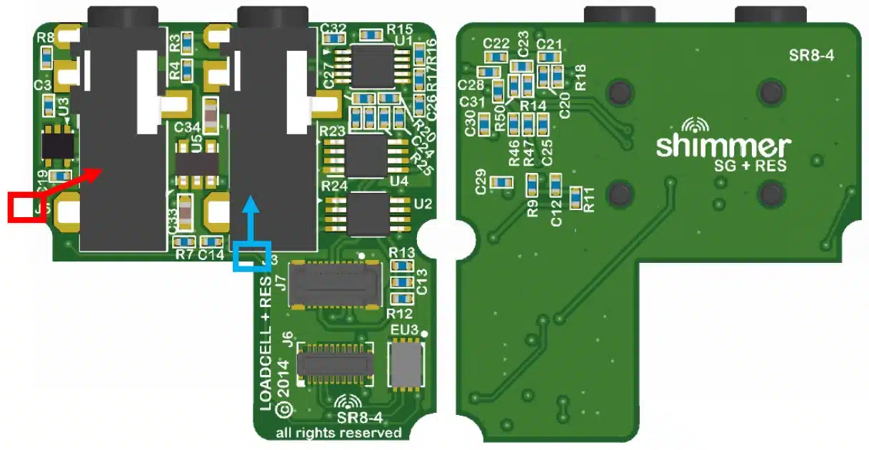
Figure 8‑1 Board Layout for Bridge Amplifier+ Expansion Board
The 3.5 mm 4-position jack connectors, J3 and J5, (indicated in Error! Reference source not found.) have four connections each, as labelled in Error! Reference source not found.. Their connections are listed in Error! Reference source not found. and Error! Reference source not found..
Figure 8‑2 Connector labels for 3.5mm 4-position jack
| Connector Pin # | Shimmer3 Label | Function / Notes |
|---|---|---|
| Sleeve (J3.1) | GND | Ground Connection |
| Tip (J3.2) | SGP | Signal (Positive) |
| Ring1 (J3.3) | SGN | Signal (Negative) |
| Ring2 (J3.4) | PV_SG | 2.8V if GPIO_INTERNAL1 is high. |
Table 8‑1 Shimmer Bridge Amplifier+ Expansion Board connections for J3.
Important Note: Do not insert a two-position 3.5mm plug into the J3 connector as this may cause a short-circuit between PV and GND.
| Connector Pin # | Shimmer3 Label | Function / Notes |
|---|---|---|
| Sleeve (J5.1) | GND | Ground Connection |
| Tip (J5.2) | SGN | RDIV1 (Signal) |
| Ring1 (J5.3) | GND | Ground Connection |
| Ring2 (J5.4) | GND | Ground Connection |
Table 8‑2 Shimmer Bridge Amplifier+ Expansion Board connections for J5.
Important Note: The pin-out of the J5 connector is not the same as that for other Shimmer3 expansion boards and is not compatible with Shimmer accessories, such as the Optical Pulse Sensing Probe.
A high quality four-position 3.5mm jack with cable is available for purchase from Shimmer. You can wire this connector to your load cell according to the connections in Error! Reference source not found..
Hardware customisation
DISCLAIMER: We recognize the variation in gain and ranges of interest when performing research with load cells. Hardware customization is best discussed with our engineers at the time of order and executed by our factory. The following information is provided to customers as-is. Please do not modify the hardware unless you have access to the proper SMT rework tools and appropriate training. Damage caused by user customization will invalidate any warranties and repairs will be estimated on a per-case basis.
Gain for the Bridge Amplifier Low gain output can be reduced by 2 by adding a 360k .1% resistor across R8. Other values are not recommended.
Gain for the Bridge Amplifier High gain output can be adjusted by replacing R25 or paralleling a resistor on R3. Gain = 1 + (R3/180k).
The Bridge Amplifier unipolar output can be shifted positive (for bi-polar load cells) by replacing or placing another resistor across R47. R47 is normally 300k, 100k will result in a zero-output voltage of ~1.5V
R7 (200k)is the pull-up for the Resistance Amplifier. The part can be removed for active sensors or changed to best match a specific variable resistance transducer.
R8 (zero-Ohm jumper) connects the Resistance Amplifier to ground. Replacing with a fixed resistance may allow a shift in transducer output if a reduction in signal range is acceptable.
Gain for the Resistance Amplifier can be adjusted by replacing R13 (1.0M) or paralleling a resistor on R13. Gain = 1 + (R13/110k)
Troubleshooting – secure connection between Shimmer and expansion board
For any device purchased on or after September 1st, 2014, the Bridge Amplifier+ Module is permanently fixed to the Shimmer3 mainboard. Removal of the expansion board from the mainboard should not be carried out under any circumstances. Doing so will cause damage to one or both of the boards and any necessary repairs will not be covered by warranty.
For devices purchased before September 1st, 2014, it was possible to disconnect the Bridge Amplifier+ Module from the Shimmer3 mainboard. For these devices, Shimmer recommends an adhesive to secure the connection between the Shimmer3 mainboard and Expansion Boards. The adhesive that is used by Shimmer during assembly is called Superdots (www.superdots.com). We use the Ultra Tak variety. With Superdots applied, the expansion boards can still be removed and swapped out, if required, as the adhesive does not go solid but has a rubbery consistency, allowing it to be removed. However, customers should remember that frequently removing expansion boards is not recommended and can cause damage to the connectors. Superdots also provides some shock absorbtion.
Shimmer fits the Superdots by stretching them around the edges of the Expansion Board. This ensures that the adhesive doesn’t prevent the connectors from making a good connection and there is enough adhesive to secure the boards together but not to interfere with the fit. Note: Shimmer does not supply Superdots.
8.2. Opening the Shimmer3 expansion enclosure
Whilst the Shimmer3 enclosures can be opened to allow users to change the SD card, it is important to note that the plastic enclosures are not designed for regular opening and closing. In particular, it is recommended that the screws not be removed and reinserted on a regular basis as damage to the plastic by over-use of the screw mechanism will occur. Furthermore, the expansion board connectors can be damaged by disconnecting and reconnecting, resulting in the loss of communication with the expansion board.
For (legacy) devices purchased between September 2014 and January 2016, the Bridge Amplifier+ Module will be permanently fixed to the Shimmer3 mainboard. Removal of the expansion board from the mainboard should not be carried out under any circumstances. Doing so will cause damage to one or both of the boards and any necessary repairs will not be covered by warranty.
For (legacy) devices purchased before September 1st, 2014, it is possible to disconnect the Bridge Amplifier+ Module from the Shimmer3 mainboard. Please note, however, that this is not recommended.
Whether the BA+ Unit is permanently fixed to the Shimmer3 mainboard or not, if the enclosure must be opened to replace the SD card, care must be taken not to damage the expansion board connection, which could result in loss of communication between the expansion board and the Shimmer3 mainboard. Please refer to the Shimmer assembly video on our YouTube channel4.
8.3. Recommended accessories
Philips 21091A Technical Data
Please follow this link5, register and search for the Philips 21091A skin-surface temperature probe for more information, which is recommended for use with the Resistance Amplifier input of the Shimmer Bridge Amplifier+ Unit. This skin temperature probe can be purchased on the Shimmer e-store6.
The following approximate resistance values have been measured by Shimmer:
| Temperature (°C) | Resistance (kΩ) |
|---|---|
| -18 (approx – freezer) | 16.8 |
| 10 | 9.3 |
| 26 | 4.5 |
| 37 (approx – body temp) | 1.5 |
| 80 | 0.55 |
Table 8‑3 Shimmer Bridge Amplifier+ Expansion Board connections for J5.
The accuracy of the probe is quoted as ± 0.1 °C (25-45 °C), ±0.2 °C (0-60 °C).
Shimmer performed an in-house calibration of the resistance amplifier output with the Philips 21091A skin-surface temperature probe inserted using Vernier’s Direct-Connect Temperature Probe7. Shimmer found the relationship between the resistance amplifier channel output and temperature in °C to be logarithmic. To convert the resistance amplifier output from mV to °C based on Shimmer’s in-house calibration, apply the following formula:
y = -27.42ln(x) + 56.502
Where y = temperature in °C
Where x = (200*Vo)/((10.1)Pv-Vo)
Where Pv = 3000mV
Where Vo = Uncalibrated output of the resistance amplifier channel
Note: For a more accurate resistance to temperature (°C) conversion users are advised to calibrate the resistance amplifier output against two temperature measurement systems.
8.4. How to Connect a Wheatstone Bridge to the Shimmer Bridge Amplifier
A full bridge arrangement is used for connecting strain gauges and measuring strain. Section 2.2 lists the input signal range.
Based on the deflection of your sensor you will want to choose resistance values to best match with our front end gain:
Normal channel: ±7mV, ±2.5mV/V
High Gain channel: 0-4mV, ±1.43mV/V
In general use, you should use the highest resistor values that you can as they lower system power consumption but you need to consider the equivalent resistance of your pressure sensor.
Referring to Error! Reference source not found. and Error! Reference source not found., the top/bottom of the bridge would go to the PV_SG/GND signals and the output would be SIGP/SIGN.
It is recommended that users review the principles of bridge operation using online resources. The following serves as a good introduction: http://www.sensorland.com/HowPage004.html.
Calculated specification, exact value subject to environmental and component variation.↩︎
The Excitation source is software controlled.↩︎
This value is load-cell dependant, to estimate use the formula I = 1 + 2.8/(RSGin || RSGout); RSG data is available from the load-cell manufacturer.↩︎
https://estore.healthcare.philips.com/b2b_store/b2b/z_init.do↩︎
http://www.shimmersensing.com/shop/skin-surface-temperature-probe#related-tab↩︎
http://www.vernier.com/products/sensors/temperature-sensors/dct-din/↩︎
Legal notices
Legal Notices and Disclaimer
Redistribution IS permitted provided that the following conditions are met:
Redistributions must retain the copyright notice, and the following disclaimer. Redistributions in electronic form must reproduce the above copyright notice, this list of conditions and the following disclaimer in the documentation and/or other materials provided with the document.
Neither the name of Shimmer Research, or Realtime Technologies Ltd. nor the names of its contributors may be used to endorse or promote products derived from this document without specific prior written permission.
THIS DOCUMENT IS PROVIDED BY THE COPYRIGHT HOLDERS AND CONTRIBUTORS “AS IS” AND ANY EXPRESS OR IMPLIED WARRANTIES, INCLUDING, BUT NOT LIMITED TO, THE IMPLIED WARRANTIES OF MERCHANTABILITY AND FITNESS FOR A PARTICULAR PURPOSE ARE DISCLAIMED. IN NO EVENT SHALL THE COPYRIGHT OWNER OR CONTRIBUTORS BE LIABLE FOR ANY DIRECT, INDIRECT, INCIDENTAL, SPECIAL, EXEMPLARY, OR CONSEQUENTIAL DAMAGES (INCLUDING, BUT NOT LIMITED TO, PROCUREMENT OF SUBSTITUTE GOODS OR SERVICES; LOSS OF USE, DATA, OR PROFITS; OR BUSINESS INTERRUPTION) HOWEVER CAUSED AND ON ANY THEORY OF LIABILITY, WHETHER IN CONTRACT, STRICT LIABILITY, OR TORT (INCLUDING NEGLIGENCE OR OTHERWISE) ARISING IN ANY WAY OUT OF THE USE OF THIS DOCUMENT, EVEN IF ADVISED OF THE POSSIBILITY OF SUCH DAMAGE.
